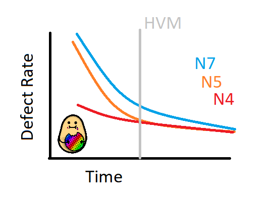
𝐷𝑟. 𝐼𝑎𝑛 𝐶𝑢𝑡𝑟𝑒𝑠𝑠 on X: Here's a mockup of what was shown regarding TSMC's N4 D0 defect rate compared to previous nodes. Grey line shows high volume manufacturing start (N4 beyond HVM
By A Mystery Man Writer

TSMC OIP Forum: Fabs, N3/N2+BSPN - by Dr. Ian Cutress

Better Yield on 5nm than 7nm': TSMC Update on Defect Rates for N5
𝐷𝑟. 𝐼𝑎𝑛 𝐶𝑢𝑡𝑟𝑒𝑠𝑠 on X: Here's a mockup of what was shown regarding TSMC's N4 D0 defect rate compared to previous nodes. Grey line shows high volume manufacturing start (N4 beyond HVM

TSMC OIP Forum: Fabs, N3/N2+BSPN - by Dr. Ian Cutress

OGAWA, Tadashi on X: RT @IanCutress: OK, here's my full set of $TSM graphs. ➡️ TWD rev up ($613B to $625B) ➡️ but TWD:USD is also up ➡️ so USD revenue Q4

More Than Moore, Dr. Ian Cutress
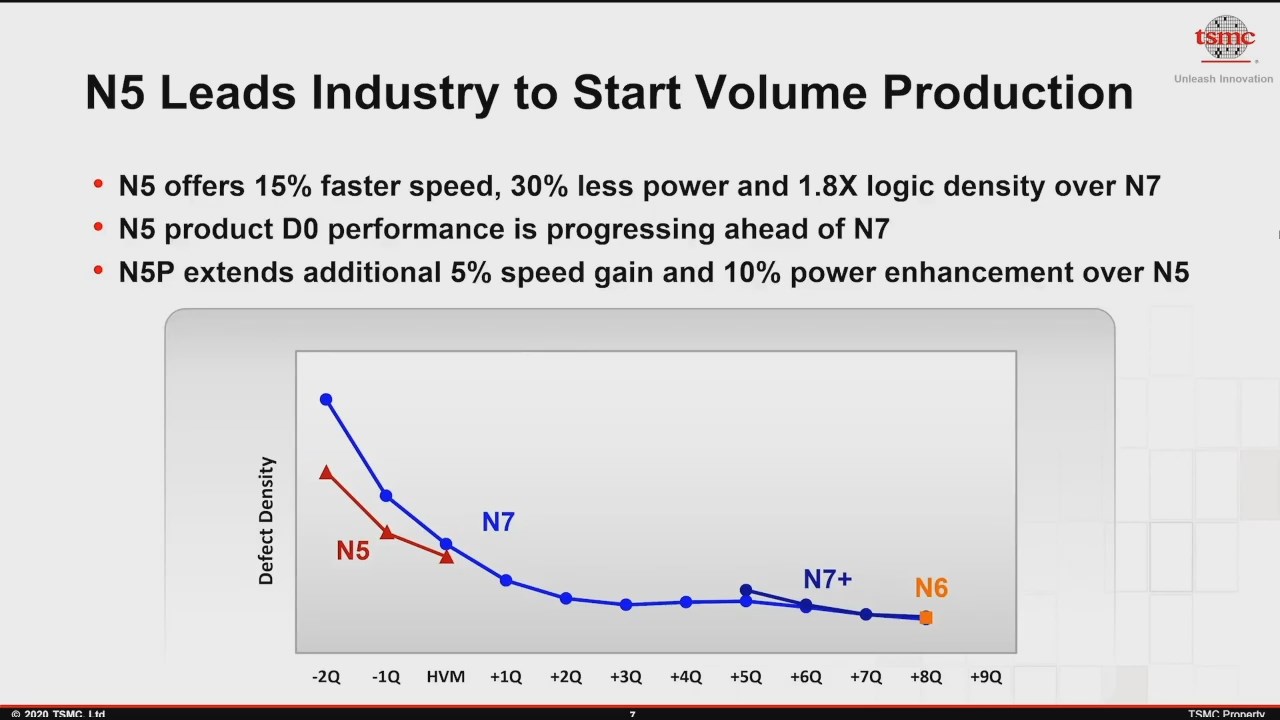
Better Yield on 5nm than 7nm': TSMC Update on Defect Rates for N5
TSMC OIP Forum: Fabs, N3/N2+BSPN - by Dr. Ian Cutress

TSMC OIP Forum: Fabs, N3/N2+BSPN - by Dr. Ian Cutress

TSMC OIP Forum: Fabs, N3/N2+BSPN - by Dr. Ian Cutress
Better Yield on 5nm than 7nm': TSMC Update on Defect Rates for N5
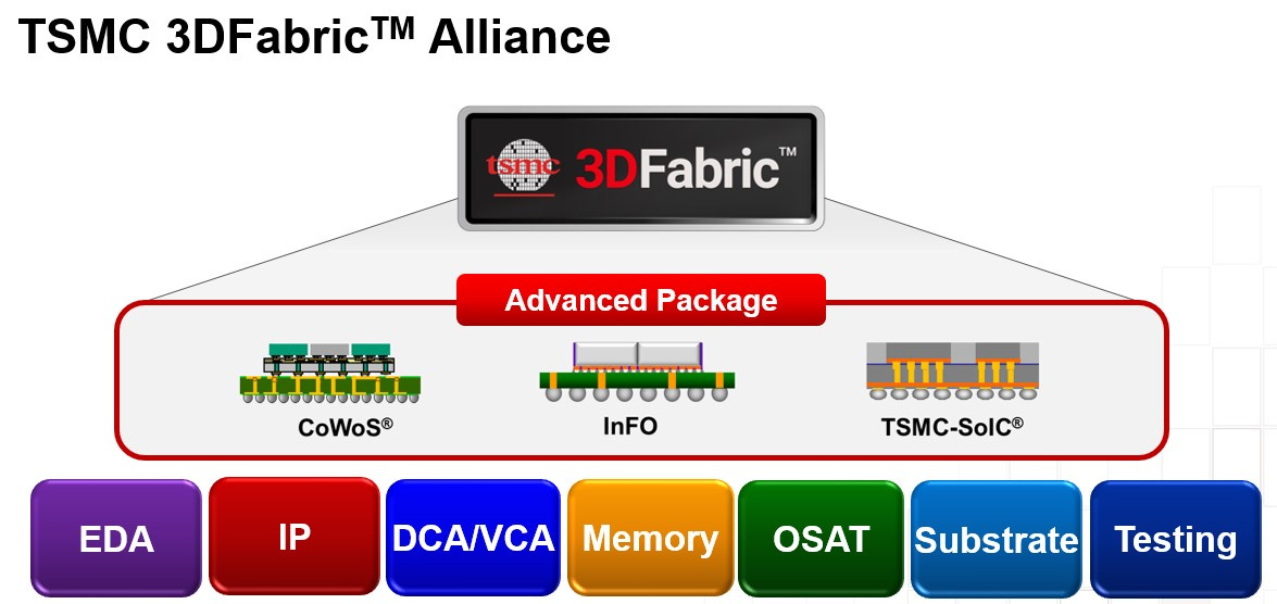
TSMC OIP Forum: Fabs, N3/N2+BSPN - by Dr. Ian Cutress

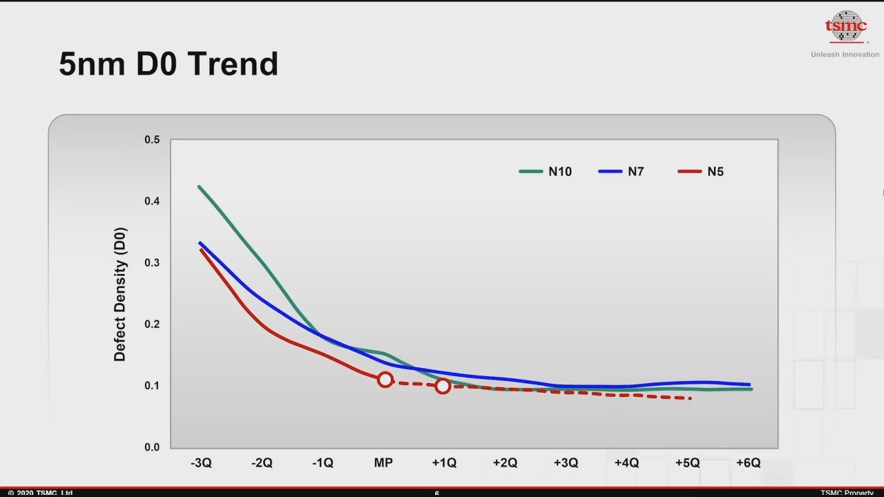
𝐷𝑟. 𝐼𝑎𝑛 𝐶𝑢𝑡𝑟𝑒𝑠𝑠 on X: Even if the D0 defect rate was 7 per square centimeter (or 100x worse D0 than TSMC's N7 which is 0.07), yield would be 87.55% on a