By A Mystery Man Writer


Warren FLACK, Vice President, PhD
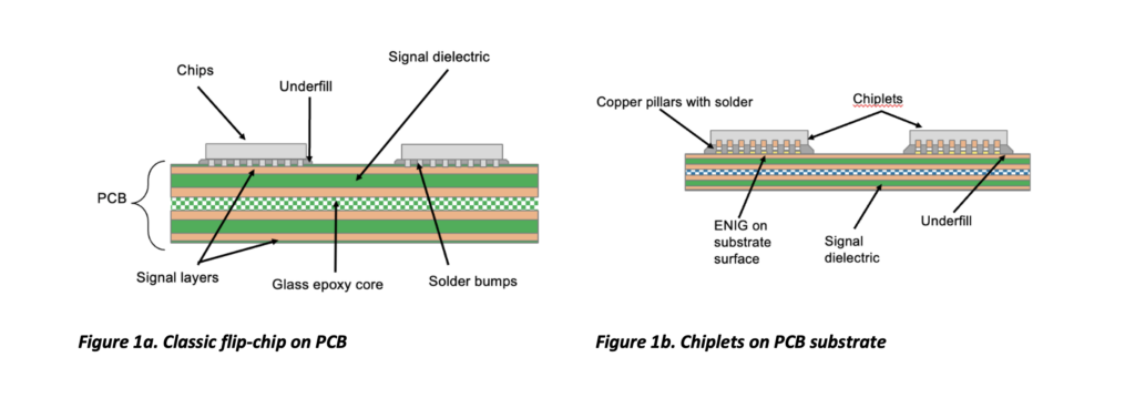
Optimizing Chiplet Packaging for Complex Applications - QP Technologies

Redistribution in wafer level chip size packaging technology for high power device applications: Process and design considerations - ScienceDirect
RDL and Flip Chip Design

Schematic structure of FBTI.
Redistribution Layer (RDL) Technology for ICs Package

Figure 1 from Integrated 122-GHz Antenna on a Flexible Polyimide Substrate With Flip Chip Interconnect
_en.png)
redistribution layer (chip) (RDL)
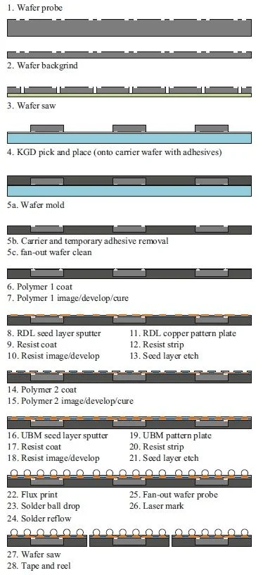
Polymers in Electronics Part Six: Redistribution Layers for Fan-Out Wafer Level Packaging - Polymer Innovation Blog
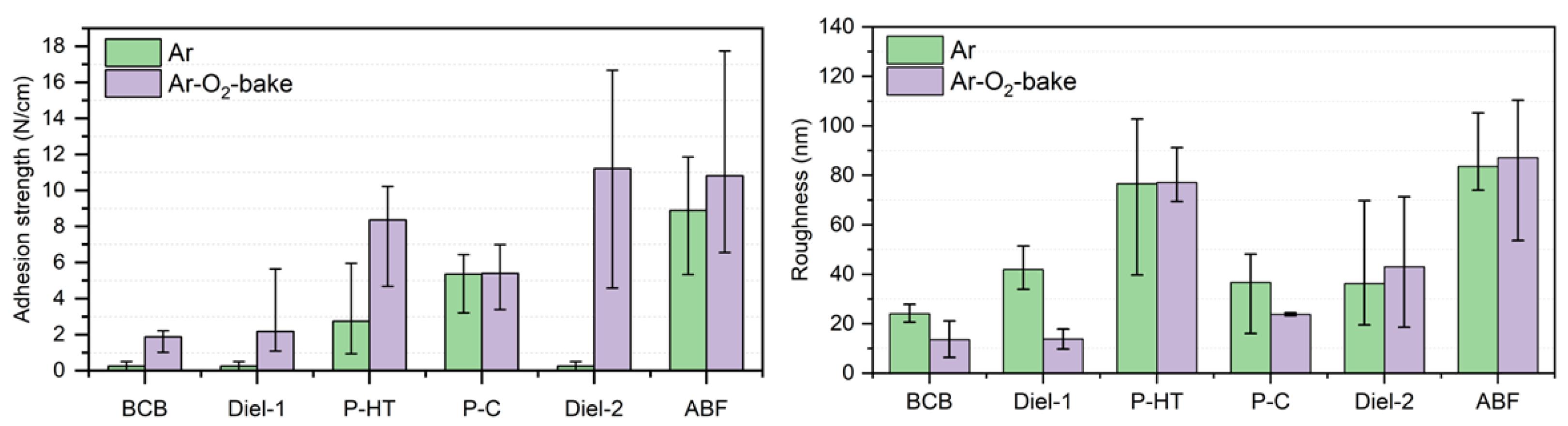
Polymers, Free Full-Text
Advanced Semiconductor Engineering, Inc. WLCSP Design Guide

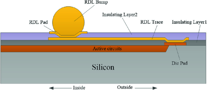
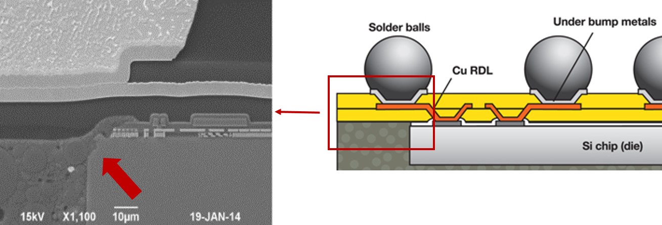
The bond pad redistribution layer (polyimide 1) and the under bump

The bond pad redistribution layer (polyimide 1) and the under bump

Polymers, Free Full-Text